Glass targets AI packaging

Glass substrates are emerging as a potential alternative to organic packaging materials as AI accelerators require larger packages with higher chiplet and HBM integration density.
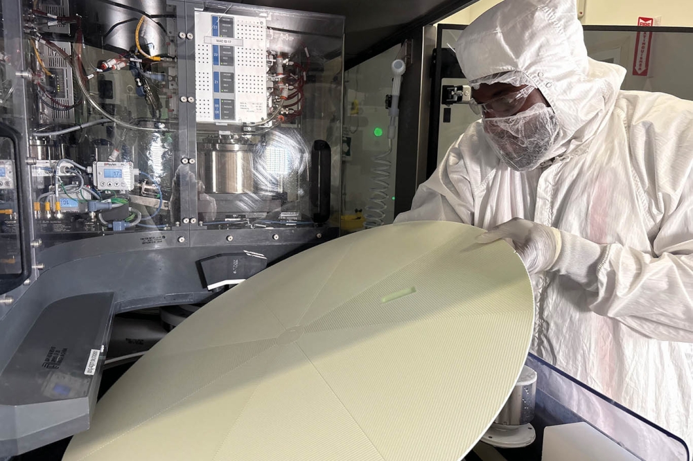
The semiconductor industry is increasingly exploring glass core substrates and glass interposers for advanced AI and high-performance computing packages, where conventional organic substrates are facing challenges related to size, warpage and interconnect density.
AI accelerators are integrating growing numbers of chiplets and high-bandwidth memory (HBM) stacks, pushing package dimensions beyond 70–100mm per side.
The thermal expansion mismatch between organic substrates and silicon can contribute to warpage, solder-joint stress and alignment challenges during manufacturing.
Glass offers greater dimensional stability, with a coefficient of thermal expansion closer to that of silicon. Manufacturers can also form through-glass vias (TGVs) through the material and build fine copper wiring across its surfaces, providing a route to higher interconnect density.
Industry estimates suggest glass substrates could support significantly more interconnects within the same area than conventional organic substrates, potentially enabling larger and denser packages for AI accelerators and data-centre processors.
Several major semiconductor companies are developing the technology. Intel has demonstrated large glass-based packages through its R&D programmes, while Samsung Electro-Mechanics and LG Innotek are developing glass substrate technologies through pilot production. TSMC is also working on glass-panel packaging.
However, commercialisation remains challenging. Glass is brittle, creating risks of cracking during drilling, processing and dicing, while maintaining high manufacturing yields at larger panel sizes remains a key challenge. The supply chain for specialised low-expansion glass is also relatively concentrated.
The technology is currently largely at the pilot-production stage, with limited-volume applications expected to emerge around 2028. As AI packages continue to grow in size and complexity, glass substrates could become an important technology for supporting higher-density chiplet and HBM integration.