Researchers at the Institute of Science Tokyo have developed BBCube, a next-generation semiconductor integration platform that combines advanced chip packaging, high-density interconnects and thermal management to address key challenges in AI hardware.
The platform integrates three core technologies: a proprietary high-density chip-on-wafer (COW) process, bumpless chip interconnection technology and a multiscale thermal analysis method, supporting advanced 2.5D and 3D heterogeneous integration for AI accelerators and high-performance computing systems.
BBCube uses via-last through-silicon vias (TSVs) to connect chips without conventional metal bumps, enabling finer-pitch interconnects and reducing chip-to-chip spacing to 10 μm.
According to the researchers, the architecture has the potential to deliver up to 16 times greater aggregate signal bandwidth within the same interconnection area while maintaining signal quality comparable to conventional micro-bump designs.
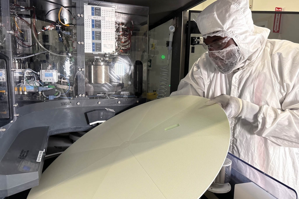
To address heat generation in densely integrated packages, the team also developed a waffle wafer structure that reduced thermal resistance by approximately 52% in simulations.
A complementary multiscale thermal analysis technique enables heat distribution across an entire chip to be evaluated at 1 μm resolution using 100 million analysis points.
Together, the three technologies form a unified platform designed to support compact, high-performance AI systems with improved connectivity, efficient cooling and scalable heterogeneous integration.
The researchers believe BBCube could help accelerate the development of future AI accelerators and high-performance computing devices as semiconductor packaging complexity continues to increase.