Multi-die packaging drives 2nm scaling

Advanced packaging, chiplets and heterogeneous integration are becoming increasingly important as semiconductor scaling moves to 2nm and below, driven by the demands of AI and high-performance computing.
Multi-die assemblies are becoming increasingly central to leading-edge semiconductor design as traditional transistor scaling struggles to deliver the performance and efficiency gains required by AI workloads.
According to industry experts cited by Semiconductor Engineering, chiplets and advanced packaging are enabling manufacturers to combine multiple processing elements within larger, more complex systems, while continuing to use different process nodes for different functions.
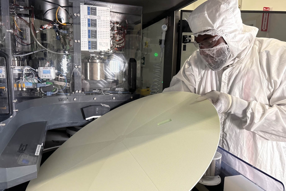
The shift is also driving demand for larger interposers. ASE has highlighted a roadmap extending from 5.5-reticle packages towards 9X, 12X and potentially 40X interposer sizes. Larger interposers, however, increase package cost and introduce new manufacturing and reliability challenges.
Alternative interposer technologies are therefore gaining attention. Organic and glass interposers are being developed as lower-cost alternatives to silicon, while high-density redistribution layers and bridge architectures offer additional approaches to connecting multiple dies.
Chiplet integration remains another major focus. Although chiplets have been used commercially for more than a decade, the industry is still working through challenges around interoperability, standards, cost and reuse. The lack of a mature chiplet marketplace means many current multi-die systems remain highly customised.
Thermal management is becoming increasingly important as package power and utilisation rise. Industry approaches include liquid cooling, microchannels, cold plates, immersion cooling, thermal vias and emerging two-phase cooling technologies. Thermal and mechanical considerations are also increasingly being incorporated into package and system design from the outset.
At the same time, advanced simulation and machine learning are being used to optimise increasingly complex manufacturing and packaging processes. Virtual models and digital twins can help engineers evaluate materials, process conditions and thermal behaviour before committing to physical prototypes.
As semiconductor manufacturing moves towards 2nm and below, the combination of continued transistor scaling with multi-die integration, advanced interconnects, larger interposers and new thermal solutions is expected to become increasingly important for delivering the performance-per-watt improvements demanded by next-generation AI systems.