Building standards for the next era of advanced packaging

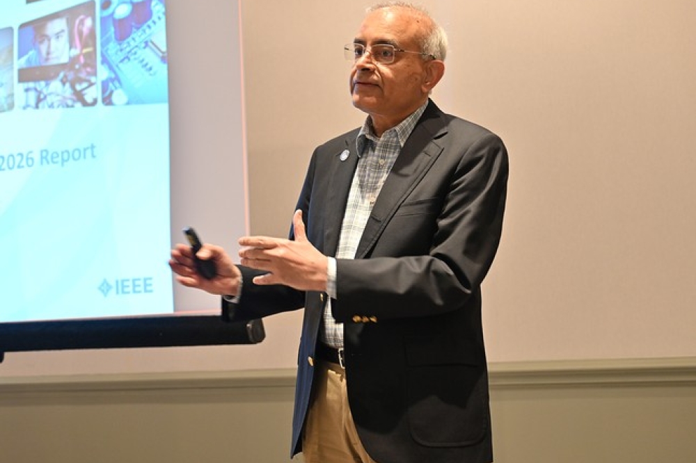
AP Magazine Editor Sarab Chopra speaks with Peter O’Brien,
Head of Photonics Packaging at Tyndall National Institute, about how
standardisation, chiplets and photonic-electronic integration are shaping the
future of advanced packaging.
As semiconductor architectures become increasingly complex, advanced packaging is emerging as a critical technology enabling the next generation of high-performance computing, AI infrastructure and photonic-electronic integration. From chiplets and advanced interposers to thermal management and digital modelling, the industry is moving towards highly integrated solutions that require new approaches to design, manufacturing and collaboration.
Advanced Packaging Magazine Editor Sarab Chopra, spoke with Peter O’Brien, Head of Photonics Packaging at Tyndall National Institute, to discuss Tyndall’s role in advancing semiconductor packaging, the importance of standardisation, how pilot lines are helping bridge the gap between research and manufacturing, and the technologies shaping the future of advanced packaging.
SC: For readers who may be unfamiliar with Tyndall, could you introduce the organisation and explain your role in advanced packaging?
POB: Tyndall is based in Cork, Ireland, and is primarily a semiconductor research centre. We work across wafer fabrication, semiconductor design, packaging, reliability testing and application development.
My area is advanced packaging, where we take semiconductor chips and develop packaging solutions for different applications. We also have significant reliability testing capabilities, allowing us to test packaged devices under different conditions and perform failure analysis.
Beyond packaging, we have application teams working across areas such as telecommunications and biomedical technologies.
A key part of Tyndall’s model is our close relationship with industry. We have several industry partners physically located on-site, including packaging equipment companies and technology providers. We also collaborate closely with major technology companies such as Meta and Intel.
The objective is to create an environment where research and industry can work together closely to accelerate innovation in semiconductor technologies.
SC: What are the current priorities for Tyndall in advanced packaging?
POB: One of our biggest priorities is standardisation.
When we established the packaging group around 15 years ago, we quickly recognised a significant opportunity because many areas, particularly photonics, were highly customised.
Integrated photonics, whether based on silicon photonics or indium phosphide technologies, has traditionally been very bespoke. The customer often defines the entire ecosystem around their specific application requirements.
That flexibility is useful during early-stage technology development, but it becomes a challenge when you want to scale. Scaling requires standards, similar to what has enabled the semiconductor industry to grow.
Our focus has been moving towards more standardised approaches in design, fabrication and packaging.
One example is the development of packaging building blocks, which we refer to as Assembly Design Kits, or ADKs. They are similar in concept to Process Design Kits, or PDKs, used in semiconductor foundries. The objective is to create validated and repeatable processes that address the majority of users while still allowing customisation when required.
By following standards, companies can reduce costs, shorten development timelines and enter the ecosystem more easily.
SC: How important is the convergence of photonics and electronics for the future of advanced packaging?
POB: This is one of the most important developments happening today.
Historically, photonics has often been treated as a separate technology domain with its own ecosystem. However, integrated photonics increasingly needs to become part of the wider microelectronics landscape.
By aligning photonics with electronics, we can benefit from the scale of the semiconductor industry, including manufacturing infrastructure, equipment, workforce expertise and established supply chains.
We are already seeing major semiconductor foundries and technology companies incorporating photonics into their roadmaps. The industry is moving towards a future where photonics technologies are manufactured and integrated within semiconductor environments.
Photonics will not replace electronics, but it provides significant advantages in areas such as bandwidth, performance and energy efficiency.
The challenge now is identifying the most important technologies, standardising them and integrating them into the semiconductor ecosystem so they can scale effectively.
SC: Scaling technology from research into manufacturing remains a major challenge. How does Tyndall help bridge that gap?
POB: Pilot lines are designed specifically to bridge the gap between research and industrialisation.
A technology may be successfully demonstrated in a research environment, but commercialising it requires a much broader ecosystem. Companies, particularly SMEs, often struggle to access the infrastructure, expertise and supply chains needed to scale.
Historically, pilot lines focused on demonstrating that hundreds or thousands of components could be manufactured. However, what we have learned is that a successful pilot line needs to do more than manufacture parts, it needs to build an ecosystem.
That means bringing together material suppliers, equipment providers and industrial partners.

For example, if we are developing new substrates, the objective is not necessarily for Tyndall to manufacture those substrates ourselves. Instead, we want industry partners to become part of the supply chain and help establish a scalable manufacturing route.
The same applies to equipment. Packaging equipment is often highly customised, but more standardised manufacturing tools will be essential as the industry grows.
Ultimately, scaling is not only about producing larger volumes. It is about creating the environment that allows industry to scale successfully.
SC: How does Tyndall collaborate with industry partners, and what support do companies typically seek?
POB: The first step is engagement. Semiconductor technology is a global industry, so we spend significant time travelling, meeting companies and understanding their challenges.
A major part of our role is communicating the importance of ecosystem development, standardisation and supply chain creation.
When companies approach us, they often have a product concept but may not have deep expertise in areas such as packaging. They may ask: How should we approach this design? Which manufacturing route should we follow? Which suppliers should we work with?
Our role is not simply to package devices for them. Instead, we guide them towards established processes and connect them with the right industrial partners.
Training is also a very important part of our work. Many companies need their workforce to understand advanced packaging technologies, even if they ultimately outsource manufacturing to an OSAT.
They need engineers who understand the technology well enough to evaluate suppliers, manage manufacturing relationships and ensure requirements are being met.
SC: What trends do you see as most transformative in advanced packaging?
POB: There are several major trends shaping the future of advanced packaging.
The first is the continued integration of photonics and electronics. Technologies such as co-packaged optics require photonics manufacturing processes to become compatible with semiconductor manufacturing environments.
The goal is not to create separate photonics factories, but to enable photonics technologies to be manufactured within existing semiconductor ecosystems.
Another major trend is the rise of chiplet architectures.
Instead of creating one very large chip containing every function, systems are increasingly being divided into smaller chiplets manufactured using different processes and then integrated together.
This requires advanced interconnect technologies and increasingly sophisticated interposers. Materials such as silicon, glass and hybrid substrates are becoming increasingly important.
Thermal management is another major challenge. As package densities increase, managing heat becomes essential for maintaining performance and reliability.
Heat affects electrical performance, optical alignment, mechanical stability and long-term reliability. Developing new thermal materials and cooling approaches will therefore be critical.
SC: How is Tyndall addressing energy efficiency and sustainability in advanced packaging?
POB: One important area is the development of digital twins for semiconductor packages.
A digital twin combines the physical characteristics of a real-world package into a comprehensive model. For advanced packaging, this means modelling multiple physical domains simultaneously, including thermal, optical, electrical and mechanical behaviour.
These domains are highly interconnected. A change in temperature can affect mechanical expansion, optical alignment and electrical performance.
Using multi-physics modelling, we can predict how changes in materials or designs will influence the complete system before manufacturing begins.
This is particularly valuable when companies consider alternative materials or more sustainable substrate options. Instead of relying on trial and error, they can simulate the impact of different choices.
With advances in AI and machine learning, these models are becoming increasingly powerful, allowing companies to predict both technical performance and manufacturing outcomes.
Cost modelling is another important development. Companies need to understand not only whether a technology works, but whether it can be manufactured economically at scale.
By modelling different manufacturing routes, companies can make better decisions before committing significant investment.
SC: What future breakthroughs or milestones in advanced packaging are you most excited about?
POB: One exciting area is the move towards surface-level optical packaging.
Traditionally, optical fibres connect at the edge of a chip in a one-dimensional arrangement. However, future systems will require optical connections on the top surface of chips, similar to how electrical connections are already arranged.
Moving to two-dimensional optical arrays will significantly increase optical I/O density, which is essential for future AI systems requiring enormous data movement.
Another important development is advanced interposer technology.
Future chiplet-based architectures will require thousands of high-density interconnects between different semiconductor devices.
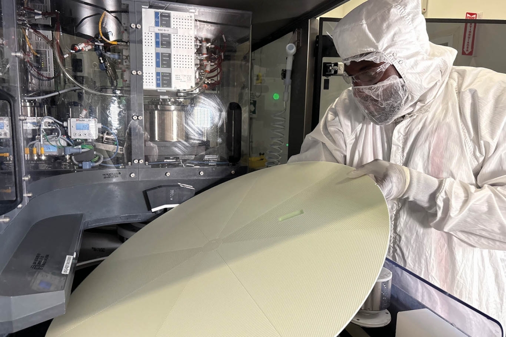
Glass interposers are particularly interesting because they can potentially use large panel processing techniques, similar to those developed for flat-panel display manufacturing.
This could enable very large, high-volume packaging solutions for applications such as AI data centres, where package sizes continue to increase.
SC: What is the long-term vision for Tyndall’s role in advanced packaging?
POB: The long-term goal is to help create a scalable and globally competitive ecosystem for advanced packaging.
That means developing standardised technologies, connecting research with industry, supporting supply chain development and ensuring companies have access to the skills and infrastructure required.
Advanced packaging is becoming central to the future of semiconductor technology. By bringing together photonics, electronics, materials, manufacturing and modelling, we can enable the next generation of high-performance computing systems.