Rapidus expands advanced packaging roadmap

Rapidus is advancing a large-format packaging roadmap aimed at supporting next-generation AI and high-performance computing systems through larger interposers, panel-level processing and chiplet integration.
Rapidus is expanding its advanced semiconductor packaging plans, with the company targeting eight-reticle-size interposers by around 2030 as demand for AI and high-performance computing drives the need for increasingly complex chip integration.
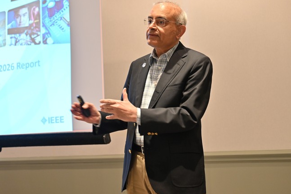
Speaking at the 2026 OCP APAC Summit, Rozalia Beica, Chief Technology Officer for Packaging at Rapidus Design Solutions, outlined a roadmap that includes progressively larger interposers, moving from four reticles covering approximately 3,320 mm² to six reticles at 4,980 mm² and ultimately eight reticles spanning 6,640 mm².
The company is also developing a 600 × 600 mm panel-level packaging platform, with the associated organic substrate expected to reach approximately 14,400 mm² by the end of the decade.
Rapidus is pursuing both conventional 300 mm wafer processing and larger panel formats. The company estimates that an eight-reticle-size interposer could produce four units on a 300 mm wafer, compared with 49 units on a 600 × 600 mm panel, highlighting the potential manufacturing and productivity benefits of moving to larger formats.
The packaging strategy is closely tied to Rapidus' chiplet roadmap. Its Rapidus Chiplet Solutions pilot line is being brought into full operation to validate 2.xD and 3D packaging technologies, while the company continues development of panel-level redistribution-layer packaging for high-density chiplet integration.
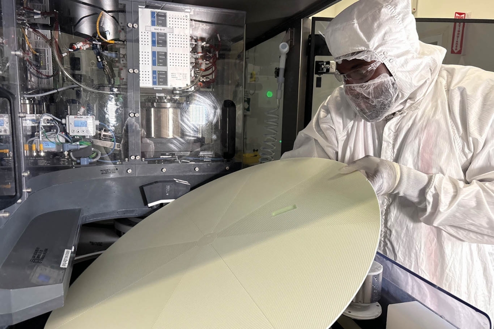
Rapidus is also collaborating with Lam Research on panel-level packaging processes. The work includes 2.xD packaging using redistribution layers on 600 mm-square glass carriers, with Lam Research's Kallisto electroplating system involved in the process. Rapidus previously unveiled a large-format glass interposer prototype and has targeted commercial production from 2028.
The company's wider packaging portfolio is expected to cover flip-chip BGA, 2.5D silicon interposers, panel-level organic interposers, bridge-based and bridge-free architectures, and 3D chip stacking using hybrid bonding.
By 2030, Rapidus expects advanced computing platforms to increasingly combine sub-2nm logic, high-bandwidth memory, chiplets, optical interconnects, hybrid bonding and panel-level packaging.
The roadmap reflects the industry's shift toward system-level scaling as conventional transistor scaling becomes increasingly challenging.