Empowering advanced FCBGA substrate design rules for automotive applications

Autonomous systems are forcing substrate design into new territory. As copper traces shrink, reliability becomes the real battleground for next-generation automotive packaging.
By Jaimal Williamson, Texas Instruments
Historically, semiconductor packaging had a moniker as the
stepchild of the semiconductor ecosystem, with back-end assembly and packaging
processes relegated as an afterthought or modest necessity for innovation,
especially when compared to front-end wafer fabrication processes that embodied
Moore’s law and high technological investment. Now, back-end packaging has
risen like a phoenix and taken its place within the semiconductor pantheon as a
quintessential differentiator, along with the Internet of Things and artificial
intelligence (AI). High-density interconnect routing enabled through flip-chip
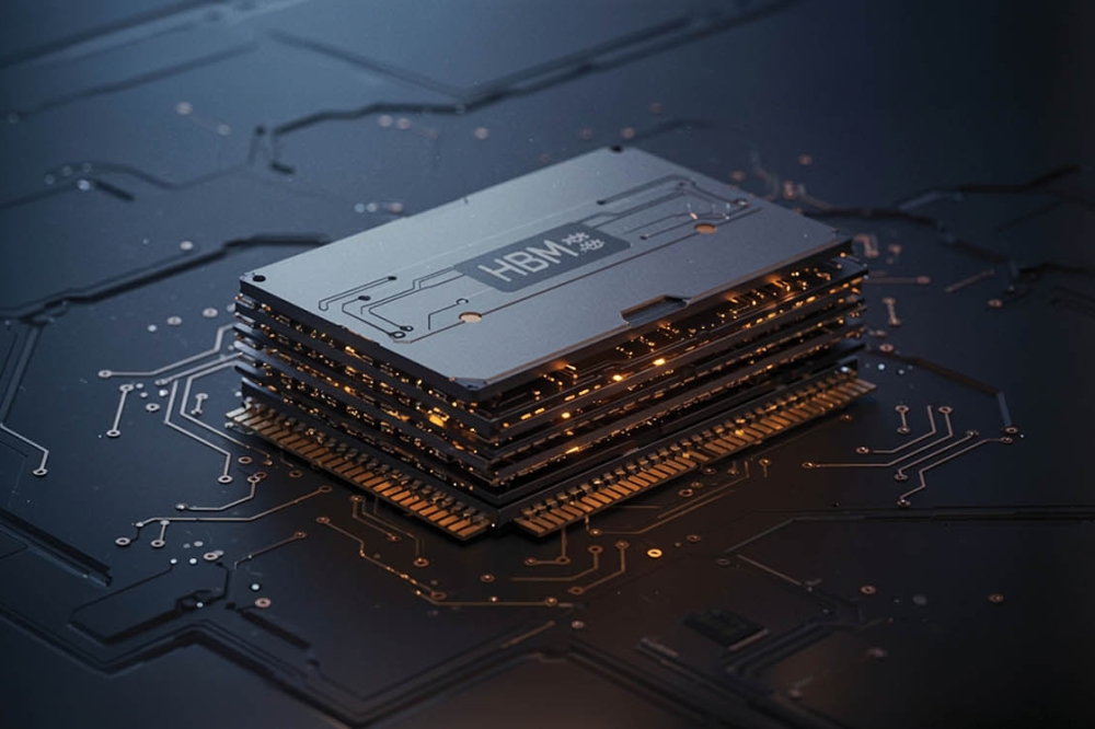
ball grid array (FCBGA) substrates (Figure 1) is now commonplace to meet
trillions of operations per second (TOPS) in devices.
For example, devices with high electrical functionality
combine serializer/deserializer and double-data-rate memory technologies,
laying the groundwork for high-density interconnects routed in substrates for a
myriad of applications. Applications supporting AI, autonomous driving,
aerospace and space, data center networking, and high-performance computing
(HPC) require TOPS to satisfy demanding operational specifications. Advanced
packaging design rules (that is, routed in FCBGA substrates) maximize interconnect
density through the distribution of fine copper (Cu) traces and spaces (the
distance to adjacent flip-chip bond pads or traces), augmenting electrical
performance. Ultimately, implementing advanced FCBGA substrate design rules can
significantly impact silicon entitlement, package form factor and cost.

Figure 1:
Example of an FCBGA package
Advanced substrate design rules can push the boundaries of substrate supplier capabilities where latent process defects or shifts can impact package assembly manufacturing and reliability yields. For example, Cu traces yielded at the low end of the width specification can present challenges of low crack resistance during temperature cycling because of a reduced cross-sectional area [1] and local coefficient of thermal expansion mismatches. On the other hand, Cu traces that yield at the high end of the width specification can present obstacles during temperature-humidity-bias testing, since a wider trace is closer to an adjacent trace or pad. This scenario increases the potential for ion migration.
Understanding the impact of advanced substrate design rules
during component-level reliability (CLR) and board-level reliability (BLR)
becomes even more paramount for automotive applications. With Tier 1 suppliers
and original equipment manufacturers driving the enviable requirement of zero
defects for automotive applications, a challenge for packaging engineers is to
dig deep into the fundamentals of materials science. This entails understanding
the chemical structure-to-transient material property relationships of organic
material sets to thermomechanical changes in various metallic material
properties within the package construction.

Figure 2:
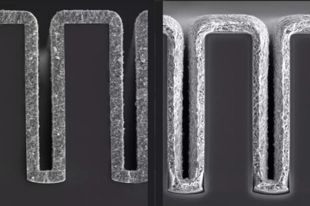
Example of a copper trace crack during temperature cycling
Examining the implementation of advanced FCBGA package
design rules in literature and across substrate supplier and outsourced
semiconductor assembly and test roadmaps, the proliferation of devices
featuring finer Cu lines and space for automotive devices is lacking. For
example, high-performance FCBGA devices such as 2.5D devices that use
high-density routing through organic or silicon interposers for HPC
applications are not subjected to the more stringent qualification conditions
defined by the Automotive Electronics Council (AEC) Q-100 standard [2].
High-interconnect-density substrate routing is a prerequisite for FCBGA package
design in order to power the demand for ultra-functionality on silicon and
packages supporting different levels of driving automation.

Table 1:
Evaluation legs subjected to package reliability testing
As higher levels of driving automation increase from Society
of Automotive Engineers J3016 standard Levels 2 and 3 (advanced driver
assistance systems) to Level 4 and 5 (autonomous driving), the implementation
of advanced substrate design rules becomes necessary to accommodate TOPS in
devices. Yet there is a gap in exploring advanced substrate designs featuring
finer Cu trace lines and space for automotive applications.

Figure 3:
Failure probability vs. first cycle to failure for legs 1 (above) and 2 (below)

For this reason, Texas Instruments conducted a detailed
study to extract package-level reliability data empirically. The study focused
on FCBGA package reliability to understand the risks associated with finer Cu
lines and space from an automotive chip-to-package interaction readiness
standpoint. The reduced cross-sectional area of fine Cu lines make it
susceptible to cracking under temperature-cycling environments (Figure 2). The
Cu lines (or traces) are typically sandwiched between a silica-filled polymeric
Ajinomoto build-up film-based dielectric material, where differences in
coefficient of thermal expansion drive stress at the internal FCBGA substrate
layers in temperature-cycling environments. Performing both board and component
temperature cycling enables full quantification of the reliability margins of
fine Cu trace routing.

Figure 4:
Failure analysis of Cu trace cracking at the inner substrate layer
Results and discussion
Performing both component- and board-level stress testing enabled a comprehensive perspective of the reliability of advanced design rules listed in Table 1. Employing an aggressive hammer test for CLR testing initiated an accelerated response based on an understanding of failure modes. This hammer test included a sequential series of aggressive moisture-soak-as-preconditioning substitute, multiple reflows at peak lead-free temperatures, and temperature cycling beyond condition B (–55°C to 125°C). BLR testing was based on Joint Electron Device Engineering Council (JEDEC) JESD22-A104 condition G, soak mode 4 conditions [3]. Recorded BLR failures occurred while in-situ monitoring after the first interruption for a period of a specified nanoseconds and an increase in daisy-chain resistance, followed by multiple additional interruptions within a percentage of the first cycles to failure.
Subjecting an equal sample size for legs 1 and 2 to the CLR hammer test conditions correlated to the failure mode produced from extended testing of typical AEC Q-100 temperature cycle condition B, and thus could accelerate the accumulation of test failures. After test failures at three different temperature cycle read points, a Weibull analysis quantified the performance between legs 1 and 2. As indicated in Table 1, the only difference in the substrate design is the Cu trace width and space. With this being the case, the cross-sectional area of the Cu trace played a significant role in the CLR results.
For leg 1, the first cycle to failure was 3.5 times earlier
than leg 2. Figure 3 shows the failure probability at a 95% confidence interval
at first cycles to failure between legs 1 and 2. The figure also highlights the
comparative results with similar failure probability plotted at a 95%
confidence interval. The failure mode in both cases was Cu trace cracking at a
similar inner layer of the substrate. Figure 4 shows the failure of the Cu
trace crack.

Figure 5:
Characteristic life at 63.2% fails for leg 1
With respect to characteristic life (alpha) and shape
parameter (beta) values, the statistics of legs 1 and 2 provide a degree of
clarity on the implications of the advanced substrate design rule of finer Cu
traces as width reduces. Per Figure 5, leg 1 shows a slope (beta is greater
than one, but less than four) that is not as steep as leg 2 (see Figure 6),
indicating earlier wear out, higher variation and a lower degree of
predictability. Leg 2 results represent a steeper slope (where beta is greater
than four), indicating a more predictable and consistent life span for this
failure mode given its wider Cu trace cross-sectional area. The beta value for
leg 2 aligns with fatigue or an aging mechanism.

Figure 6:
Characteristic life at 63.2% fails for leg 2
Figure 6 shows the characteristic life plot for leg 2. The tangible differences in slope between legs 1 and 2 are conspicuous, and therefore provide an explanation for the performance differences in characteristic life as observed in Figures 5 and 6.
Measuring warpage at both 30°C and 250°C revealed the
contribution of package warpage and Cu density, if any, as a function of the
different advanced substrate design rules between legs 1 and 2. These
temperatures provide a contrast in warpage at room temperature and peak reflow
temperature as associated with a lead-free surface-mount technology (SMT)
process. Figure 7 shows that there was not any statistical difference between
legs 1 and 2 based on overlap of circles from the JMP plot. When unmounted parts
(parts not constrained to the printed circuit board) undergo temperature
cycling, the package is free to conform to its natural state. As such,
measuring warpage upon heating and cooling at 30°C captured any hysteresis
effects and thermomechanical changes of the organic material sets as they
surpassed their glass transition temperature. Similar to the results in Figure
7, the measurements in Figure 8 show no statistical difference between legs 1
and 2 upon heating and cooling.
Evaluating legs 1 and 2 at JEDEC standard JESD22-A104
condition G, soak mode 4 conditions during BLR complements the CLR results
previously reported. Similarly, Weibull analysis was the primary metric to
quantify reliability performance between the two FCBGA advanced package rule
designs as presented in Table 1. As expected, leg 1 failed first due to the
reduced cross-sectional area of the Cu trace width. Failure analysis confirmed
Cu trace cracking.


Figure 7:
Comparison of package warpage between legs 1 (above) and 2 (below) at 30°C and
250°C
Although not reported in this study, multiple nets were
monitored in-situ during BLR, with a separate net designed to isolate
second-level interconnect reliability at BGA connections. The net reported in
this study, as extracted from in-situ BLR monitoring, corresponds to a
continuous loop path from the BGA pad through the package and first-level
connection and routed back to the BGA pad. This net was also monitored for
package integrity including Cu trace reliability.


Figure 8
(above): Comparison of package warpage of leg 1 (above) and 2 (below) heated
and cooled to 30°C
Leg 1 failed approximately 1.2 times earlier than leg 2 at
first cycles to failure. Figure 9 illustrates the characteristic life at 63.2%
fails for legs 1 and 2 under BLR testing. Comparing Figure 9a and 9b, leg 2 has
approximately 1.53 times higher cycles to failure than leg 1 at 63.2% fails.


Figure 9 (right):
Characteristic life at 63.2% fails for legs 1 (above) and 2 (below) under BLR
conditions
Similar to the CLR results, the beta value (greater than four) post-BLR testing for leg 2 aligns with fatigue or an aging mechanism. Leg 1 has a beta value less than four, which is consistent with it having earlier first cycles to failure. Again, the reduced cross-sectional area of the finer Cu trace produced with leg 1 parts is likely the reason for the earlier first cycle to failure.
Substrate suppliers typically have a Cu trace width tolerance of approximately ±2µm, where inherent manufacturing variation plays a role in the characteristic life of the distribution of parts. Nonetheless, both BLR and CLR results show high margin in meeting AEC Q-100 conditions.
Conclusion
This study demonstrated the efficacy of advanced FCBGA design rules compatible with specific Cu trace width and space values and material sets through BLR and CLR conditions. Extracting package-level reliability margins befitting higher levels of driving automation was the focal point of this empirically based study.
The study subjected an equal distribution of FCBGA parts to accelerated CLR based on an understanding of common failure modes generated during standard AEC Q-100 conditions and BLR at JEDEC standard JESD22-A104 condition G, soak mode 4 conditions, tested to device failure. Weibull analysis provided suitable statistics to understand the wear-out mechanism of the Cu trace crack failure mode.
As anticipated, the finer Cu trace parts (leg 1) exhibited the first cycles to failure. The Weibull shape parameter (beta) value of less than four was consistent with the early cycles to failure that occurred during CLR and BLR testing, coupled with a wider variation of parts failing.
Given the reduced cross-sectional area of the Cu trace and its impact on reliability margin, packaging engineers must go the extra mile in understanding substrate supplier process control because of its contribution to chip-to-package (CPI) interaction. Studying the effects of CPI by measuring package warpage across a lead-free SMT profile found no statistical differences.
Developing an automotive mindset to achieve zero defects requires constructive interaction across substrate suppliers, assembly sites and material suppliers, coupled with a strong discipline canvassing literature. For the latter task, there is usually a precedent to set a path for exploration and deeper learning. The crux is empowering advanced substrate design rules as an inevitable feature of flip-chip packaging to facilitate higher levels of driving automation.
Acknowledgment
The author would like to acknowledge Lee McNally for his input on Weibull analysis.
Jaimal Williamson is a Packaging Engineer and Senior Member
Technical Staff within Texas Instruments’ Packaging Technology Solutions group,
Dallas, TX, USA. His focal areas as a lead technologist include flip-chip
platform development of advanced CMOS Si nodes, qualification, and
productization to support multiple automotive, industrial, aerospace, and
defense applications. He has authored and co-authored 35+ journal articles,
conference papers, and technical magazine articles, as well as 35+ U.S. patents
in the field of semiconductor packaging. He received a BS in Chemistry from
Grambling State University and a MS in Polymers (via School of Materials
Science and Engineering) from the Georgia Institute of Technology.