Precision, reliability and integration in advanced packaging

As advanced packaging technologies evolve to support AI
accelerators, chiplet architectures and photonic-electronic integration, the
industry is facing mounting challenges around nanoscale alignment, thermal
management and long-term reliability.
By Sarab Chopra, Editor, Advanced Packaging Magazine
As AI infrastructure scales and semiconductor architectures become increasingly heterogeneous, advanced packaging is rapidly emerging as one of the industry’s most strategically important enabling technologies. Discussions throughout AP International 2026 demonstrated how packaging is no longer viewed as a secondary assembly process, but as a central determinant of system performance, manufacturability and long-term reliability.
The growing adoption of chiplet-based architectures, co-packaged optics, 2.5D and 3D integration, fan-out wafer-level packaging and hybrid bonding is fundamentally reshaping manufacturing requirements across the semiconductor ecosystem. These architectures promise substantial gains in bandwidth density, power efficiency and system-level integration, but they also introduce unprecedented assembly and reliability challenges.
A recurring message from speakers was that advanced packaging is increasingly inheriting the precision requirements traditionally associated with front-end semiconductor fabrication. Overlay tolerances are shrinking from microns to nanometres, while package architectures are becoming far more thermally and mechanically complex. The result is that packaging engineers are now confronting problems that span optics, materials science, motion control, thermal engineering and reliability physics simultaneously.
Heterogeneous integration drives new alignment demands
One of the strongest themes at the conference was the growing importance of heterogeneous integration. Combining logic dies, memory, photonic integrated circuits, ASICs and advanced substrates into tightly integrated packages is allowing semiconductor companies to overcome some of the scaling limitations associated with traditional monolithic device architectures.
However, this transition is dramatically increasing assembly complexity.
Presentations from PI (Physik Instrumente) highlighted how modern heterogeneous systems require sub-micron alignment between optical, electrical and mechanical interfaces. In many advanced packaging configurations, even extremely small positioning errors can significantly degrade performance.
This becomes especially critical in silicon photonics, where optical waveguides may only measure 150–200nm in width. At these dimensions, sub-micron positional deviation can produce insertion losses that exceed device operating margins. The challenge becomes even greater when coupling multi-channel fibre arrays, where all optical paths must be optimised simultaneously while compensating for vibration, thermal drift and process variation.

Speakers repeatedly stressed that conventional passive alignment approaches are becoming insufficient for next-generation packaging flows. Instead, the industry is moving toward active alignment systems capable of continuously adjusting positioning in real time using optical or electrical feedback signals.
These systems increasingly rely on six-degree-of-freedom positioning platforms capable of controlling X, Y and Z translation as well as rotational correction. The ability to dynamically compensate for mechanical movement, thermal expansion and curing-induced stress is becoming essential for maintaining coupling efficiency and production yield.
Packaging evolves into a precision engineering discipline
The conference repeatedly reinforced the idea that packaging is evolving into a front-end-like precision manufacturing discipline.
In traditional semiconductor assembly, packaging tolerances were comparatively forgiving relative to lithography and wafer fabrication processes. That distinction is rapidly disappearing.
Hybrid bonding and wafer-level integration are pushing overlay requirements into the nanometre regime. Wafer-to-wafer bonding processes now target overlay accuracy below 200nm across full 300mm wafers, while die-to-wafer assembly systems are being expected to achieve throughput exceeding 1,000 units per hour without compromising placement precision.
This transition is forcing manufacturers to rethink motion control, metrology and assembly architectures.
Presenters described how advanced alignment platforms increasingly combine long-range servo stages with piezoelectric nanopositioners capable of sub-nanometre resolution. Closed-loop capacitive sensors are being integrated directly into assembly systems to continuously monitor and correct drift during operation.
Flexure-guided nanopositioners, parallel-kinematic hexapods and hybrid coarse/fine positioning architectures are becoming increasingly important because they eliminate backlash, minimise friction and improve long-term repeatability. Some systems now integrate firmware-level optimisation algorithms capable of autonomously identifying optimal coupling positions in milliseconds.
The increasing sophistication of these positioning systems reflects the growing difficulty of maintaining process stability at advanced packaging scales.
Hybrid bonding introduces new manufacturing challenges
Hybrid bonding emerged as one of the most technically demanding areas discussed during the event.
As semiconductor manufacturers pursue higher interconnect density and lower power consumption, hybrid bonding is becoming increasingly attractive for next-generation chiplet integration. However, these processes introduce substantial assembly complexity.
Presenters explained that thermal compression bonding generates thermo-mechanical drift during assembly, requiring active compensation throughout the bonding cycle. High-density bump arrays with pitches below 40µm leave effectively no tolerance for placement error, while wafer bow and local substrate warpage further complicate alignment.

The challenge becomes even greater in multi-die and multi-material systems. Differences in coefficient of thermal expansion between silicon, glass, organic substrates and photonic materials can generate substantial stress during thermal cycling. These stresses can distort package geometry, reduce co-planarity and compromise optical or electrical interconnect integrity.
Maintaining flatness across the package substrate therefore becomes critically important. Even relatively small warpage can prevent precise optical alignment or generate stress concentrations capable of damaging fine-pitch interconnects.
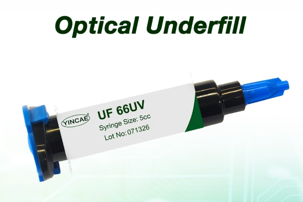
To address these issues, manufacturers are increasingly exploring low-CTE materials, advanced underfill chemistries, stiffener-ring architectures and highly controlled adhesive deposition techniques. However, presenters acknowledged that achieving acceptable yield and repeatability remains difficult as package complexity continues increasing.
Co-packaged optics increases integration density
Co-packaged optics (CPO) was another dominant topic throughout the conference, particularly as AI systems continue demanding higher bandwidth density and lower interconnect power consumption.
By placing photonic components directly alongside switching ASICs and accelerators, co-packaged optics architectures aim to overcome the bandwidth and power limitations associated with traditional pluggable optical transceivers. However, this approach substantially increases manufacturing and reliability complexity.
Presenters described how co-packaged optics systems integrate ASICs, photonic integrated circuits, fibre arrays, silicon bridges, TSV interposers and advanced substrates into highly compact assemblies requiring extreme positional accuracy.
In many cases, fibre-array placement accuracy below 0.2µm is required to maintain acceptable coupling performance. Multiple flip-chip bonding stages, high-density interconnect structures and multi-material integration further increase the risk of assembly-induced defects and reliability degradation.

TSMC’s COUPE architecture was discussed as an example of the industry’s broader effort to bring optical connectivity physically closer to compute resources. However, speakers emphasised that these architectures can only become commercially scalable if alignment automation, thermal management and manufacturing repeatability improve significantly.
The conference made clear that co-packaged optics is no longer simply a research topic. Instead, it is rapidly becoming a practical engineering challenge tied directly to future AI infrastructure deployment.
Thermal management becomes a limiting factor
Thermal management emerged as one of the most pressing constraints facing advanced packaging technologies.
The convergence of photonic devices with increasingly power-dense AI processors is creating extremely challenging thermal environments.
While modern ASICs generate substantial heat during operation, optical components remain highly temperature-sensitive and can experience performance degradation even under relatively modest thermal variation.
This creates conflicting design requirements within tightly integrated packages.
Presenters highlighted how 2.5D and 3D integration architectures further complicate thermal behaviour by increasing power density and restricting heat dissipation pathways. Vertically stacked dies, TSV structures and dense interconnect layers can all contribute to localised thermal hotspots.
As a result, conventional air-cooling strategies are increasingly viewed as insufficient for future high-performance systems.
Several advanced cooling approaches were discussed during the conference, including liquid cold-plate cooling, integrated heat spreaders and high-performance thermal interface materials incorporating graphite and boron nitride. These solutions aim to improve heat extraction while minimising thermal gradients across sensitive photonic-electronic assemblies.
However, speakers noted that thermal management is no longer simply a cooling problem. Thermal behaviour now directly affects alignment stability, package warpage, material stress and long-term reliability, making it deeply interconnected with nearly every aspect of advanced package design.
Reliability concerns grow for harsh-environment applications
Beyond manufacturability and throughput, reliability remained a major area of concern throughout the conference.
Presentations from Tyndall National Institute focused heavily on the environmental stresses faced by advanced packages operating in harsh conditions such as aerospace and defence applications.
Space-qualified systems may experience severe thermal cycling, radiation exposure, vacuum operation, mechanical shock and high-frequency vibration simultaneously. These environments create major challenges for both electronic and photonic assemblies.
Researchers outlined extensive qualification methodologies involving thermal shock, temperature cycling, humidity exposure, vibration analysis, vacuum testing and radiation evaluation. Accelerated stress testing is increasingly being used to identify potential failure mechanisms before deployment.

Particular attention was given to the evaluation of automotive-grade commercial off-the-shelf (COTS) components for possible space applications. Automotive-qualified devices offer attractive cost and availability advantages compared with traditional space-grade components, and early testing results showed encouraging reliability performance across several evaluated devices.
However, photonic systems remain significantly more difficult to qualify for harsh environments.
Photonic packaging introduces unique reliability risks
Unlike conventional electronic assemblies, photonic devices are highly sensitive to positional stability and environmental contamination.
Conference presentations highlighted several reliability risks associated with photonic packaging, including cracked optical elements, solder-joint degradation and vibration-induced fibre damage following environmental stress testing.
Hermetic sealing remains one of the industry’s most persistent challenges. Many photonic modules contain organic materials that can outgas under vacuum conditions, potentially contaminating optical surfaces and degrading long-term performance.
At the same time, delicate optical structures are vulnerable to thermo-mechanical stress caused by coefficient-of-thermal-expansion mismatch between package materials. Even relatively minor dimensional changes can disrupt optical alignment.
Presenters also noted that photonic systems frequently contain brittle glass structures and precision fibre assemblies that are especially susceptible to vibration and shock damage. Maintaining alignment stability over long operational lifetimes therefore remains a major qualification challenge for photonic packaging technologies.
As optical integration density increases, these reliability concerns are expected to become even more difficult to manage.
Economics and scalability remain major barriers
While much of the conference focused on technical capability, production economics emerged as an equally important discussion point.
Several presentations emphasised that alignment processes are becoming one of the largest contributors to photonic manufacturing cost. In some photonic assembly flows, alignment alone may account for as much as 80% of total device cost.
This creates major scalability concerns as AI and optical interconnect deployments continue accelerating.
Traditional serial alignment methods, which may require several minutes for individual coupling operations, are incompatible with future high-volume manufacturing requirements. Reducing “cost per placement” is therefore becoming a major strategic priority across advanced packaging supply chains.
Automation is increasingly viewed as the only viable solution. Real-time feedback systems, autonomous optimisation algorithms and high-speed multi-axis alignment platforms are being deployed to reduce manual intervention while improving throughput consistency.
The industry’s broader challenge is no longer simply achieving high-performance packaging in laboratory environments. It is achieving that performance repeatedly, reliably and economically at manufacturing scale.
Packaging becomes central to future semiconductor roadmaps
A clear conclusion emerging from AP International 2026 was that advanced packaging is no longer supporting semiconductor innovation from the sidelines, it is actively driving it.
The rise of AI accelerators, optical interconnects, chiplet architectures and heterogeneous integration is fundamentally changing the relationship between packaging and system performance.
Precision alignment, thermal engineering, reliability qualification and manufacturing automation are now central to the semiconductor roadmap itself.
As package architectures continue increasing in density and complexity, the ability to simultaneously manage nanoscale precision, thermal stability, manufacturability and long-term reliability will become one of the industry’s defining competitive differentiators.
The discussions at AP International 2026 demonstrated that the future of semiconductor scaling may depend just as much on packaging innovation as on advances in transistor technology itself.